
The component is used in smart watch, mobile phone, PMP, PND…(small- sized1.8~7 inches), palm electronic apparatus, E-book (medium-sized 7~12 inches), and public information post computer, industrial work computer (large size, more than 12 inches). In application, the maximum size of the component can be up to 21 inches.
Our company Granted ISO 9001:2000 and 14001:2004 Certification.
Nano Bit Tech. to exhibit at 2014 Finetech, Japan. You are welcome to visit our booth!
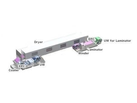
With the development in display, touch panel, solar battery, transparent electrode and electromagnetic wave shielding industries and flexible electronics, in recent years the research on and development of highly conductive and highly transparent coating and film are drawing more and more attentions. To improve the competitiveness for both our customers and ourselves and reduce production costs, Nano Bit Tech has initiatively introduced the continuous Roll to Roll coating technology and made research and development on production and manufacturing of the transparent conductive film. We have put the large-area transparent conductive films with good uniformity into production.
● Dry etching process:using laser beams directly to make dry etching, different from conventional wet complicated photolithography.● The dry etching process applied on the conductive layers, including the transparent conductive material and silver paste, removes the conductive layer with laser to achieve the aim of pattern transfer.● It is a non-masked process, featuring reduced costs, fast sample making and shortened development cycle.● It is also a one-step eco-friendly process with fast, low-temperature and energy-saving advantages.