● Dry etching process:using laser beams directly to make dry etching, different from conventional wet complicated photolithography. ● The dry etching process applied on the conductive layers, including the transparent conductive material and silver paste, removes the conductive layer with laser to achieve the aim of pattern transfer. ● It is a non-masked process, featuring reduced costs, fast sample making and shortened development cycle. ● It is also a one-step eco-friendly process with fast, low-temperature and energy-saving advantages.
Circuit design | Wet etching – Photolithography | | photoresist coating | Exposure | Develop-ing | Drying | Etching | Stripping |
- Masking is costly
- Chemical material supplying central system is required
- Waste fluid treatment system is required
- Complicated process – High-cost energy consumption
| Circuit design | Dry etching – Laser etching |
- No masking cost
- No need of central supplying system, no waste fluid
- Single process – Environment protecting and energy saving
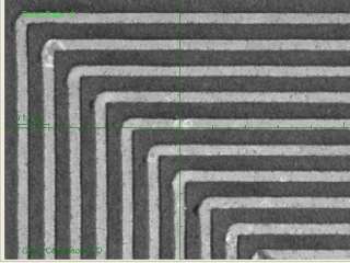 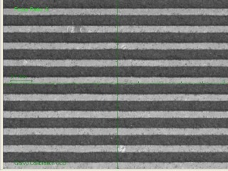
Optical microscope photo of silver wire layout 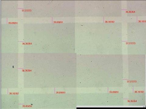
Laser etching technology can be applied on the transparent conductive layer, which is a simple yet stable and fast process.
|